DEFCON 25 HHV Challenge - Part 2: Hardware Hacking

Extracting the Firmware
At this point I tried several things such as holding down different buttons at boot up to see if we could enable the debugging output, but this had no effect. At this point I decided that I needed to see if I could dump the firmware.
Sometimes getting firmware off ROM on a microcontroller can be a really difficult task. Luckily, after looking through the datasheet of the PIC12F1572, I noticed that there is a programming mode that allows us to read the program memory. The programming section of the datasheet is a little scant on details, but refers to a separate datasheet, DS41573 which provides more detail. The first thing that stood out to me was the following:
Getting Into Programming Mode
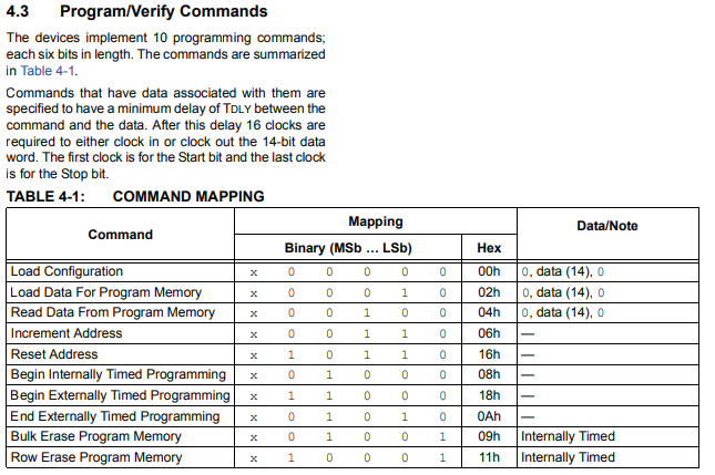
We’ll come back to this diagram later to get some details but based on this section of the programming data sheet, we should be able to read out the firmware over the programming interface. Now we just need to figure out how to do that.
Before we can start programming, we need to get into programming mode. As it turns out there are two different ways to enter programming mode:
- Low Voltage - Low voltage mode has the advantage of needing to manipulate fewer pins and you only need to deal with the operating voltage of the chip (
Vddor 3.3v - 7v). The downside to low voltage mode is that a bit can be set that disables low voltage programming mode. - High Voltage - High voltage mode will always work to enter programming mode and can also pause execution before any code runs. However, it comes with the disadvantage of needing to manipulate more pins and provide two different power sources, one at
VPPand the other atVIHH
My first attempt was to use low voltage programming mode, which was a failure. I was never able to read anything out of the device.
So high voltage it is! According to the documentation, to get into high-voltage mode we must perform the following steps:
- Hold
ICSPCLKandICSPDATlow. All other pins are unpowered. - Raise the voltage on
MCLRtoVIHH - Raise the voltage on
Vdd from 0vto the operating voltage.
This might seem a bit confusing but let’s start with the pins we need to manipulate then we’ll get to how to manipulate them.
ICSPCLK: This pin will be used as the clock signal we generate. This is the same asRA1we will drive this from a Raspberry Pi GPIO pin.ICSPDAT: This pin will be used to send our read commands as well as read the data after a command is set. We will drive this with a Raspberry Pi GPIO pin.MCLR: This isRA3. This is also used for reset, but in this case we need to provide a programming voltage. We will drive this directly from my power supply.
We’ll need to provide two different voltages:
VIHH- The data sheet says this is between 8 - 9v. This will be provided by the power supply.VDD- This is the operating voltage 3.3v - 7v. This will be provided by a Raspberry Pi GPIO pin.
In the end you get this setup: 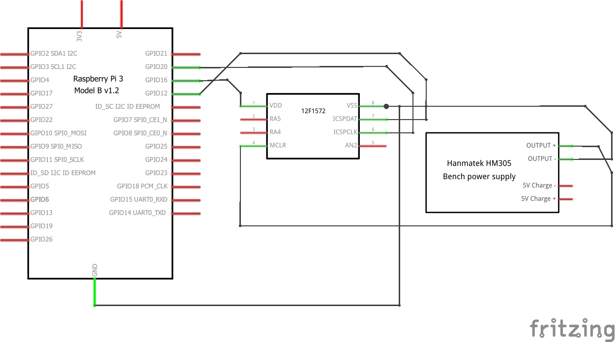
I also had a logic analyzer watching the data go in and out, which isn’t in the diagram. This helped me debug any issues and allowed me to validate my script.
Using Programming Mode
Let’s write a little code to get us into programming mode using this set up.
from time import sleep
import sys
from typing import List
from rich.progress import track
from rich import print

DELAY = 0.0001

CLK_PIN = 20
DAT_PIN = 12
POWER_PIN = 16

def main():

    signal.signal(signal.SIGINT, handler)

    if len(sys.argv) < 2:
        print("Error: You must provide an output filename.")
        sys.exit(1)

    out_file = open(sys.argv[1], "wb")

    # Set up GPIO pins.
    GPIO.setmode(GPIO.BCM)
    GPIO.setup(CLK_PIN, GPIO.OUT)
    GPIO.setup(DAT_PIN, GPIO.OUT)
    GPIO.setup(POWER_PIN, GPIO.OUT)

    print("Setting up pins...")
    GPIO.output(POWER_PIN, 0)
    GPIO.output(CLK_PIN, 0)
    GPIO.output(DAT_PIN, 0)


    print("Waiting for the go button ...")
    print("You may now power up the device to 8-9v, press enter when done.")
    sys.stdin.read(1)
    print("Going...")

    GPIO.output(POWER_PIN, 1)
    sleep(0.01)

	# We are now in programming mode.

if __name__ == "__main__":
	main()
In this code we’ve set up our clock pin, data pin and 3.3v power pin as GPIO outputs and pulled them all low. Then we wait for the user to press a button after they’ve turned on the 8-9v power supply. Once that’s done, we bring the 3.3v power pin high, entering programming mode.
But now what?
The Commands
The programming datasheet describes the process of interacting with the chip in programming mode. It follows a simple pattern where we provide a clock signal, and for the first 6 cycles we send in a 6-bit command through ICSPDAT by setting our data pin to be an output pin. At which point, we flip our data pin to be an input pin and read any response (if appropriate).
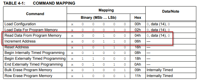
According to the chart above, we need two different commands. The first one will read out the program memory and the second will increment the address that is read.
In the case of reading the program data that would look like this:
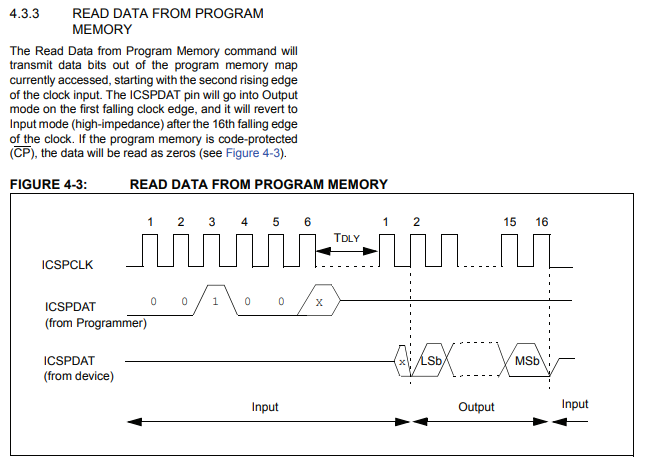
Let’s write a generic function that will toggle the clock while sending in the command that we want. Later, we’ll write the function that will read that data.
CMD_READ_DATA = (6, 0b000100)
CMD_INC_ADDR = (6, 0b000110)


def send_msg(msg):

    GPIO.setup(DAT_PIN, GPIO.OUT)
    #GPIO.output(DAT_PIN, 0)

    num_bits = msg[0]
    sequence = msg[1]


    for x in range(0, num_bits):
	    # Shift and get the next bit.
        value = (sequence >> x) & 1

		# Set the data pin to the right value.
        GPIO.output(DAT_PIN, value)

		# Raise the clock
        GPIO.output(CLK_PIN, 1)

        sleep(DELAY)

        # Lower the clock.
        GPIO.output(CLK_PIN, 0)
        sleep(DELAY)
According to the documentation the data is supposed to change on the rising edge of the clock signal and is latched on the falling edge (pg. 14). This means that we need to change our output bit as / before the clock pin goes high, and the data is “read” once that clock goes low again.
Reading the Data
This solves the first half of the problem, sending the command in. Now let’s figure out the second half, reading the data back:
def read_msg(out_file, num_bits=16) -> List:

    bits = []

    # Switch our pin to be an input pin.
    GPIO.setup(DAT_PIN, GPIO.IN)
    total_val = 0

	for x in range(0, num_bits):

		GPIO.output(CLK_PIN, 1)
        sleep(DELAY)
        GPIO.output(CLK_PIN, 0)

        # Throw out the first and last bit.
        if x < 15 and x > 0:
            val = GPIO.input(DAT_PIN)
            bits.append(val)

        sleep(DELAY)
    return bits
If you’re hawk eyed enough you might have noticed that, in my code, I drop the first bit and the last bit but the timing chart for the read command appears to indicate that we should get 15 bits out. This also confused me for a bit, the documentation says the following:

The code above doesn’t do anything special with the bits other than putting them into a python list. This allowed me to inspect the bits I was getting, to help with any debugging.
Now that we have a program that can send a command and get bits back all we need to do is put some structure around it and send in an address increment command once we have the bits we’re looking for. The final version of the code is here:
from time import sleep
import sys
from typing import List
from rich.progress import track
from rich import print

DELAY = 0.0001

CLK_PIN = 20
DAT_PIN = 12
POWER_PIN = 16

CMD_READ_DATA = (6, 0b000100)
CMD_INC_ADDR = (6, 0b000110)

def handler(signum, frame):
    print("Caught Ctrl+C, cleaning up.")
    GPIO.cleanup()


def send_msg(msg):

    GPIO.setup(DAT_PIN, GPIO.OUT)
    #GPIO.output(DAT_PIN, 0)

    num_bits = msg[0]
    sequence = msg[1]


    for x in range(0, num_bits):
        value = (sequence >> x) & 1
        GPIO.output(DAT_PIN, value)
        GPIO.output(CLK_PIN, 1)

        sleep(DELAY)
        GPIO.output(CLK_PIN, 0)
        sleep(DELAY)


def read_msg(out_file, num_bits=16) -> List:

    bits = []
    GPIO.setup(DAT_PIN, GPIO.IN)
    total_val = 0
    for x in range(0, num_bits):
        GPIO.output(CLK_PIN, 1)
        sleep(DELAY)
        GPIO.output(CLK_PIN, 0)
        if x < 15 and x > 0:
            val = GPIO.input(DAT_PIN)
            bits.append(val)
        sleep(DELAY)
    return bits


def dump_bits(bits, fp, num_bits=14):
    print(f"Dumping bits: {bits[:num_bits]}")
    final = 0
    for x in range(0, num_bits):
        val = bits.pop(0)
        final = final | (val << x)
    b = final.to_bytes(2, "big")
    fp.write(b)

def main():

    signal.signal(signal.SIGINT, handler)

    if len(sys.argv) < 2:
        print("Error: You must provide an output filename.")
        sys.exit(1)

    out_file = open(sys.argv[1], "wb")

    # Set up GPIO pins.
    GPIO.setmode(GPIO.BCM)
    GPIO.setup(CLK_PIN, GPIO.OUT)
    GPIO.setup(DAT_PIN, GPIO.OUT)
    GPIO.setup(POWER_PIN, GPIO.OUT)

    print("Setting up pins...")
    GPIO.output(POWER_PIN, 0)
    GPIO.output(CLK_PIN, 0)
    GPIO.output(DAT_PIN, 0)


    print("Waiting for the go button ...")
    print("You may now power up the device to 8-9v, press enter when done.")
    sys.stdin.read(1)
    print("Going...")

    GPIO.output(POWER_PIN, 1)
    sleep(0.01)


    bits_read = 0
    carry_over = 0

    all_bits = list()
    bits_to_dump = 14
    for x in track(range(0, 2000), description="Pulling Data..."):

        send_msg(CMD_READ_DATA)

        sleep(0.001)
        GPIO.setup(DAT_PIN, GPIO.IN)

        # Catch the data out in the logic analyzer.
        all_bits += read_msg(out_file)

        # Uncomment to see your bits fly by.
        #while len(all_bits) >= bits_to_dump:
        #    dump_bits(all_bits, out_file, bits_to_dump)
		sleep(0.001)
        send_msg(CMD_INC_ADDR)
        sleep(0.001)
    GPIO.cleanup()

if __name__ == "__main__":
    main()
Running the script generates the following output:

And the logic analyzer looks like this:
You can see where I added an extra delay between the command and the bits being read out. I did this for clarity and spent some time validating the bits by hand.

In the above screenshot the top line is the clock signal. It is six cycles followed by 16 cycles, then another 6 cycles.
If you look at just the first six clock cycles and read the data signal on the falling edge, you can decode the bits to 0b001000. The last bit can be anything, which is denoted in most documentation as an x (e.g. 0b00100x).
At this point we switch our data bit from output mode to input mode. And when we provide a clock signal, we get the bits: 0bx010111000001011.
Following that we send in a second command 0b0b01100x which is the increment address command.
Decoding The Data
After extracting the data, I took the output binary file and ran the strings command on it. Sadly this didn’t output much information. It’s possible that the strings were encoded in some way to prevent that kind of nonsense but I really expected to see something.
Even looking at it in hexdump didn’t immediately offer any clues:
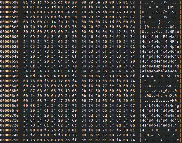
This is the point where I got a little bit confused about how to deal with this data. We’re given data 14 bits at a time, but what exactly does that mean? Do we store each opcode as a 16-bit integer, filling in the missing bits with 0? Or are we supposed to take 14 bits, and pack together those 14 bits and two bits from the next opcode to make?
Imagine if we had two instructions that were back-to-back in the firmware: CLRWDT (0b00000001100100) followed by OPTION (0b00000001100010).
You could imagine them being arranged with or without padding out to 16 bits: Unpacked:
| 31 | 30 | 29 | 28 | 27 | 26 | 25 | 24 | 23 | 22 | 21 | 20 | 19 | 18 | 17 | 16 | 15 | 14 | 13 | 12 | 11 | 10 | 9 | 8 | 7 | 6 | 5 | 4 | 3 | 2 | 1 | 0 |
|---|---|---|---|---|---|---|---|---|---|---|---|---|---|---|---|---|---|---|---|---|---|---|---|---|---|---|---|---|---|---|---|
| 0 | 0 | 0 | 0 | 0 | 0 | 0 | 1 | 1 | 0 | 0 | 0 | 1 | 0 | x | x | 0 | 0 | 0 | 0 | 0 | 0 | 0 | 1 | 1 | 0 | 0 | 1 | 0 | 0 | x | x |
Where the x is a filler bit such as 0.
Or you could imagine that there are no filler bits, and they’re packed tightly:
| 31 | 30 | 29 | 28 | 27 | 26 | 25 | 24 | 23 | 22 | 21 | 20 | 19 | 18 | 17 | 16 | 15 | 14 | 13 | 12 | 11 | 10 | 9 | 8 | 7 | 6 | 5 | 4 | 3 | 2 | 1 | 0 |
|---|---|---|---|---|---|---|---|---|---|---|---|---|---|---|---|---|---|---|---|---|---|---|---|---|---|---|---|---|---|---|---|
| 0 | 0 | 0 | 0 | 0 | 0 | 0 | 1 | 1 | 0 | 0 | 0 | 1 | 0 | 0 | 0 | 0 | 0 | 0 | 0 | 0 | 1 | 1 | 0 | 0 | 1 | 0 | 0 | n | n | n | n |
Where n is the next bits for the 3rd opcode.
This matters when we decompile the firmware and it also may be an indicator of why we don’t see any strings. If the data is tightly packed, then only some characters would end up on a byte boundary, and others would be split, giving strange results.
The datasheet doesn’t answer this question. But ultimately, I decided that the answer has to do with how the ROM on the chip works, and I’ve never heard of ROM storing weird numbers of bits.
So I decided to start with assuming they were packed as 16-bit integers as that made the most sense for how the internal ROM would work. Therefore, I decided to start by assuming they were packed as 16-bit integers.
Now comes the question of what bit order we’re supposed to store the data in. You need to look at both datasheets and you’ll notice that the data is read least significant bit first, but the opcodes in the first datasheet describing the ISA are listed with most significant bit first.

This table shows the ISA, and all the opcodes are listed with most significant bit first.
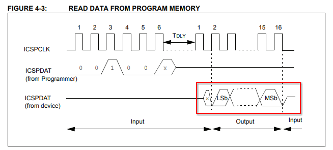
This table shows the programming interface for reading data from program memory, which gives you the data least significant bit first.
Hawk-eyed readers will have already noticed that in the code above I flipped the bits to be most significant bit first but then stored this in little endian (least significant byte first). The reason I did this was because we are going to read the data with another program which will expect the order to be in little endian.
Disassembly
At this point I made the biggest mistake of the entire project. Looking at all my favorite tools I couldn’t find any tool that would disassemble the 12F1572. Ghidra supports some PIC chips, but not the one I needed and rizin claims to handle 14-bit PIC but after digging through the source code (because I couldn’t get it to work), it turns out it’s the 14F series which is a very similar ISA with different opcodes.
But I still needed to validate that what I got out was correct, it appeared that disassembling the first 16-bits gave me a GOTO statement, so that was encouraging. I should have started writing a Ghidra SLEIGH module, but instead I decided to just write a little C++ just to do some opcode validation.
I don’t care what people say, I still love C++, that’s not where I went wrong. Where I went wrong was thinking that this would just be used for validation but instead, I ended up building a full disassembler in the end. Eventually, I was too deep into decoding opcodes that it didn’t make sense to re-write the whole thing as a SLEIGH module.
The ISA
At this point I had the ISA disassembling. But the ISA is a bit strange and requires a little explanation. If you already know the ISA, or want to learn it yourself, feel free to skip this section.
In a more common architecture such as ARM you have a certain number of what I’ll call “proper” registers. I call them “proper” registers because you can access them directly in an instruction. In ARM this would be r0 r1 r2 r3 r4 etc. The odds are you have way more registers than you could ever want. Then you have special memory addresses that allow you to access the on-chip peripherals such as UART, the interrupt controllers, timers, etc. And you usually program these by setting bits at these memory addresses.
This idea of proper registers is my own concept. I make no claims to its accuracy, validity, or consistency. It’s just how I think about it.
In the PIC12F1572 this distinction is a little bit hazier. In part this is because it’s a Harvard architecture which splits program and data memory. Additionally, the PIC only provides you with two “proper” registers: f (the file register) and W (the accumulator register). W is closer to something like an rX register in ARM, whereas the f register is always accompanied by an offset, which tells you where in memory it’s going to perform its operation. There are other ways to reference memory, but we’ll get to that later.
Here’s an example:
[72]      MOVLW       15              	; Move literal to W.
[73]      MOVLB       00              	; Move literal to BSR.
[74]      MOVWF       f:37 = W        	; Move W into F
[75]      MOVLW       4B              	; Move literal to W.
[76]      MOVWF       f:36 = W        	; Move W into F
In the above example you can see that the number 0x15 is stored in the W register, then we move W to into the memory address of f offset by 0x37.
But what is f:37? This is where things get more complicated. It depends on what memory bank is selected. In the case of the above example, we’ve selected memory bank 0x0 (instruction 73, MOVLB 00). That bank can be seen in the diagram below:
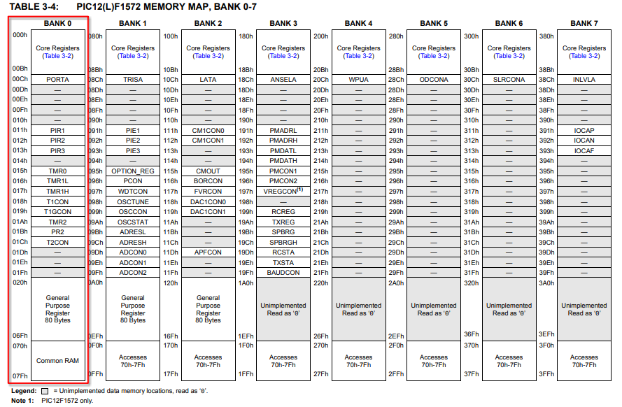
In this case the memory addresses 0x20 - 0x6F are all general-purpose memory, so the above instruction sets W to a location in general purpose memory. But if you look at the chart, you might see that all memory is not all general-purpose memory.
The first things in each bank are the set of Core Registers. You can find them below:
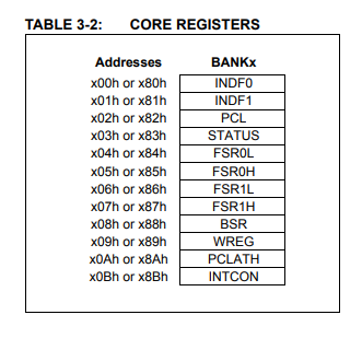
These registers are not different between banks, but every bank has the ability to refer to the same core registers for convenience. That is to say, if we set INDF0 to 0x4 in bank 0, then switch to bank 3. INDF0 is still 0x4. The same is true for the Common RAM in bank 0, is accessible by all banks.
At this point we should address that the core registers might fit my definition of a “proper” register. That’s because they do have a few instructions that deal with them directly such as
MOVLBwhich sets the BSR to some literal value. Most of the time, these instructions are going to be used indirectly by referring to them through thefregister, with an appropriate offset. Sometimes you’ll even see theWregister referred to through the use of thefregister (seen asf:WREG).
Other locations in memory are our MMIO registers that allow us to configure the on-chip peripherals. For example, in Bank 0 you can see PIR0-PIR3. PIR is the Peripheral Interrupt Register which tells you which peripheral has an interrupt. In bank 3, you can see several registers related to UART such as RCREG (Receive Register), TXREG (Transmit Register), etc. If we wanted to read or write those registers, we’d want to write some instructions such as these:
[0]      MOVLB       03              	; Move literal to BSR.
[1]      MOVF        W = f:RCREG     	; Move f
[2]      MOVWF       f:70 = W        	; Move W into F
[3]      MOVF        W = f:70        	; Move f
[4]      MOVLB       00              	; Move literal to BSR.
[5]      MOVWF       f:2B = W        	; Move W into F
In the above example:
- [ 0 ] We set the bank register to 3
- [ 1 ] We grab the most recently received character using the
fregister with the offset toRCREG, putting it into theWregister - [ 2 ] Store that value in the W register to somewhere in common RAM.
- [ 3 ] Re-read the value from where we stored it
- [ 4 ] Switch to Bank 0
- [ 5 ] Store the value we received into general purpose register bytes.
Branching is also a little strange. The PIC12F1572 has pretty typical CALL instruction and GOTO instruction but it also has conditional instructions that are dependent on the previous instruction.
Example:
[0C]      BTFSS       f:PIE1, B:RCIE == 0	; Bit Test f, Skip if Set
[0D]      GOTO        26              	; Go to address
In this example, we are testing for a particular bit to be set in the f:PIE1 register. If the bit is set, then the GOTO is skipped, otherwise if the bit is not set, the GOTO is taken. It’s equivalent to something like the following:
if (PIE1 & RCIE_MASK != 0) {
	// Do something ...
}
// Something else.
And that’s the crash course. I’ll point out anything else that’s confusing as we go along, but for now you should be able to follow the assembly.
Up Next
In part three, and armed with the knowledge of the ISA we will be finally reverse the firmware and solve the challenge!